U of A’s New Nano Lab Strengthens Pima County’s Future in Chip Manufacturing
TUCSON, Ariz. (September 9, 2025) – The University of Arizona’s latest investment in high-tech nano lab research infrastructure is taking shape, and local leaders say it could redefine Southern Arizona’s role in the global semiconductor supply chain.
In 2023, the Arizona Commerce Authority awarded the university $35 million to construct a Micro/Nano Fabrication Center on campus. On August 25, members of the Pima County Economic Development Team toured the site with Chuck Field of Kitchell Contractors Inc., the general contractor leading construction.
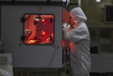
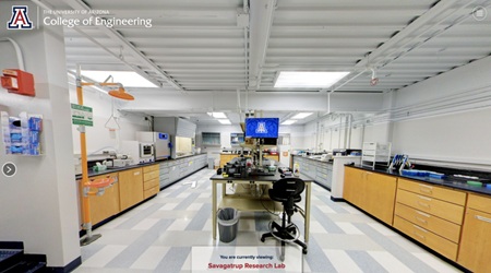
A nanofabrication center is a specialized, state-of-the-art facility that provides researchers from academia, industry, and government with access to advanced tools and clean-room environments to design, build, and test nanoscale devices and materials. The new UArizona facility will be outfitted with equipment for lithography, etching, deposition, and metrology—the same processes that drive today’s semiconductor fabs.
With the rapid rise of the semiconductor fabrication and packaging industry, the construction of this facility is more than a research investment—it is a regional economic development strategy. It enhances Pima County’s competitive edge as Arizona cements its position as a national hub for chip manufacturing and related advanced technologies.
“It was excellent to tour the facility to see what’s in store for our region and to see how we can leverage this amazing asset for Economic Development,” said Pima County Economic Development Director Heath Vescovi-Chiordi.
The center promises to create opportunities not only for university researchers but also for industry partnerships, workforce training, and startup ventures focused on next-generation chips, sensors, and advanced materials. By anchoring this research in Tucson, the U of A is helping to position Southern Arizona at the forefront of the future of chip manufacturing.
Manufacturing at the nanoscale is a global collaboration: design often originates in the United States, critical lithography equipment comes from the Netherlands (ASML’s EUV systems), raw wafers are supplied from Japan and Germany, and finished chips are produced in fabs across Asia and the U.S. Tucson’s growing research capacity helps ensure the region is tied into this worldwide ecosystem.
And it comes at just the right time. With Intel’s expansion in Chandler and TSMC’s new fabs in Phoenix, it is quickly becoming one of the premier hubs for advanced chipmaking in North America. The University of Arizona’s Nano Lab complements these multi-billion-dollar investments by providing the research backbone and talent pipeline needed to sustain the state’s growing semiconductor ecosystem.